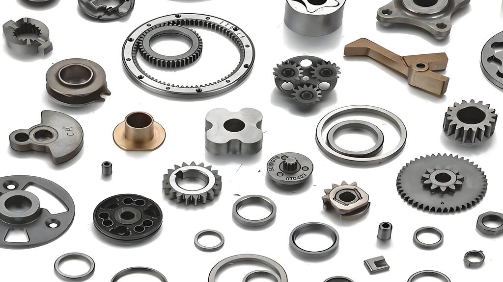


The Science Behind Ceramic Semiconductor Materials
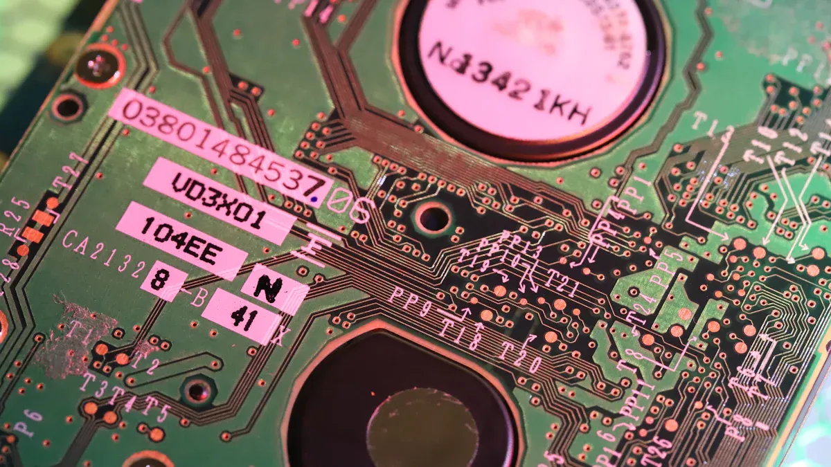
Ceramic semiconductor materials combine the durability of ceramics with the electrical properties of semiconductors, making them indispensable in modern technology. Transition metal oxides like zinc oxide exhibit semiconducting behavior, enhancing their utility in applications such as surge protection and gas sensors. These materials play a pivotal role in industries requiring precision and resilience:
- The low thermal expansion ceramics market is projected to grow from USD 4.2 billion in 2023 to USD 6.5 billion by 2032, driven by demand for thermal stress-resistant materials.
- Aerospace dominates the optical ceramics market, where high-precision components are vital for satellite systems.
- The chip multilayer ceramic capacitor market is expected to grow at a CAGR of 5.8% by 2027, reflecting their rising use in electronics.
Key Takeaways
- Ceramic semiconductors are strong and conduct electricity, making them important in tech.
- Pure ceramics improve how semiconductor devices work, making them reliable and efficient.
- Silicon carbide (SiC) is important for power electronics because it handles heat well and works at high temperatures.
- Special processing methods make ceramics purer and improve their properties.
- These materials are vital in electronics, aerospace, and optics, helping create new ideas and better performance.
Composition of Ceramic Semiconductor Materials
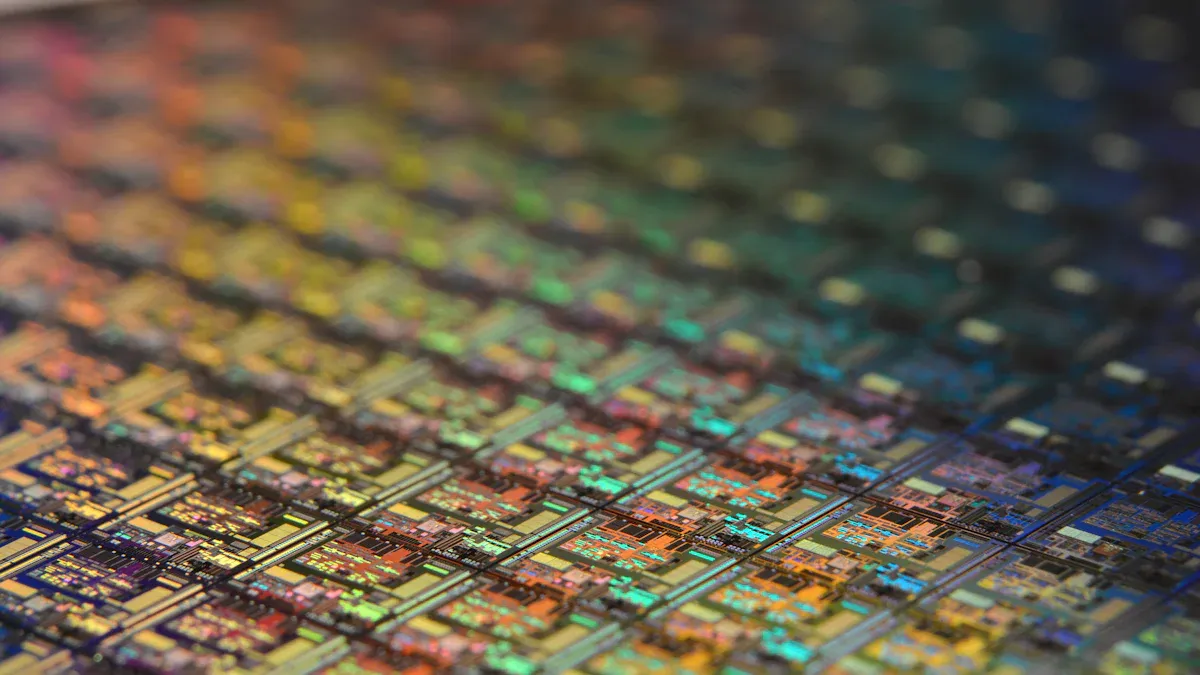
Key Elements and Compounds
Ceramic semiconductor materials derive their unique properties from specific elements and compounds. Silicon, aluminum, and zirconium are among the most commonly used elements due to their ability to form stable compounds with exceptional mechanical and electrical characteristics. For instance, silicon carbide (SiC) exhibits superior hardness and thermal conductivity, making it ideal for high-temperature applications. Similarly, silicon nitride offers exceptional strength and wear resistance, while zirconia provides high fracture toughness and thermal shock resistance.
| Ceramic Type | Key Properties | Applications in Semiconductor Manufacturing |
|---|---|---|
| Silicon Carbide (SiC) | Superior hardness, thermal conductivity, and high-temperature performance | End stations, sensors in manufacturing equiPment |
| Silicon Nitride | Exceptional strength, thermal stability, wear, and corrosion resistance | Bearings, seals, and chucks in manufacturing equipment |
| Zirconia | High fracture toughness, thermal shock resistance | Various applications in manufacturing equipment |
The choice of elements and their combinations directly influences the performance of ceramic semiconductor materials. For example, the grain size of BTS-BCN ceramics, ranging from 50–200 nm, is significantly smaller than that of traditional BaTiO3-based materials. This fine-grain size enhances dielectric strength and electrical performance, demonstrating the critical role of elemental composition in material behavior.
Oxides, Carbides, and Nitrides
Oxides, carbides, and nitrides form the backbone of ceramic semiconductor materials. Each category offers distinct advantages tailored to specific applications. Oxides like aluminum oxide (Al2O3) are known for their excellent dielectric properties and thermal stability. Carbides, including silicon carbide, excel in high-temperature environments due to their superior thermal conductivity and mechanical strength. Nitrides, such as aluminum nitride and silicon nitride, provide exceptional thermal stability and corrosion resistance, making them indispensable in semiconductor manufacturing.
- Aluminum nitride and silicon nitride are widely used in the semiconductor ceramics market for their unique properties.
- Silicon carbide stands out for its high-temperature performance and is often used in substrates and end stations.
- Aluminum oxide finds applications in optical and electronic components due to its dielectric strength.
These materials cater to specific needs within the semiconductor industry, highlighting their versatility and importance. Their performance differences stem from their atomic structures and bonding, which influence their thermal, electrical, and mechanical properties.
Purity and Material Processing
Purity plays a pivotal role in enhancing the performance of ceramic semiconductor materials. High-purity ceramics ensure better thermal stability, corrosion resistance, and electrical reliability. As the semiconductor industry advances toward smaller node sizes, such as 5nm and 3nm, the demand for high-purity materials continues to grow. This trend is further driven by emerging technologies like 5G, artificial intelligence (AI), and the Internet of Things (IoT), which require advanced ceramic components.
- High-purity ceramics improve the reliability of semiconductor devices.
- Smaller node sizes demand materials with minimal impurities to maintain performance.
- Advanced processing techniques, such as electron energy loss spectroscopy (EELS) and energy-filtered transmission electron microscopy (EFTEM), enable precise control over material composition and structure.
| Technique | Description |
|---|---|
| Electron energy loss spectroscopy (EELS) | Atomic resolution chemical and compositional analysis. |
| Energy-filtered transmission electron microscopy (EFTEM) | A family of imaging techniques to enhance, map, and quantify elements and chemicals in an image with nanometer resolution. |
| Spectrum imaging | Systematic method to generate a spatially resolved distribution of EELS data. |
| Energy dispersive x-ray spectroscopy (EDS/EDX) | Useful to elucidate elemental or chemical characterization of a sample. |
| Electron backscatter diffraction (EBSD) | Helps examine the crystallographic orientation or texture of materials. |
Material processing techniques ensure that ceramic semiconductor materials meet the stringent quality requirements of modern technology. These methods allow manufacturers to achieve the desired purity levels and optimize the properties of the final product.
Technical Properties of Ceramic Semiconductor Materials
Dielectric Strength and Electrical Conductivity
Ceramic semiconductor materials exhibit exceptional dielectric strength and electrical conductivity, making them indispensable in advanced electronic applications. Dielectric strength refers to a material's ability to withstand high electric fields without breaking down, while electrical conductivity determines how efficiently it can transport electric charge. These properties are influenced by the material's composition, structure, and purity.
For instance, the Ba0.75Ni0.25Tc0.88Mn0.12O3 perovskite ceramic demonstrates how elemental composition and conduction mechanisms impact electrical conductivity. The intrinsic characteristics of the dielectric material, combined with the electrode-dielectric interface, play a crucial role in determining performance. Energy dispersive spectroscopy (EDS) analysis confirms that the absence of impurities and adherence to stoichiometric expectations are vital for achieving optimal conductivity. This highlights the importance of precise material engineering in enhancing the electrical properties of ceramic semiconductors.
Moreover, experimental data shows that elastic strain mapping can optimize these materials' properties. By using first-principles calculations and machine learning, researchers have identified stability regions in a six-dimensional strain space. This approach reveals how reversible elastic strain can significantly alter lattice thermal conductivity, further enhancing the electrical performance of ceramic semiconductor materials.
Thermal Stability and High-Temperature Resistance
Thermal stability and high-temperature resistance are critical for ceramic semiconductor materials, especially in applications involving extreme operational conditions. These materials maintain their structural integrity and performance under high thermal stress, making them ideal for aerospace, electronics, and industrial manufacturing.
Raman spectroscopy provides valuable insights into the thermal stability of these materials. This technique identifies crystalline phases and polymorphs by detecting vibrational modes. It also reveals internal stresses through shifts in Raman peaks, which are essential for understanding mechanical strength and thermal behavior. Such analyses ensure that ceramic semiconductors can withstand prolonged exposure to high temperatures without degradation.
For example, silicon carbide (SiC) and aluminum nitride (AlN) are widely recognized for their superior thermal conductivity and stability. These materials excel in environments where conventional semiconductors fail, such as in power electronics and high-frequency devices. Their ability to resist thermal shock and maintain performance under extreme conditions underscores their importance in modern technology.
Hardness and Mechanical Durability
The hardness and mechanical durability of ceramic semiconductor materials set them apart from other materials used in advanced applications. These properties ensure that the materials can endure mechanical stress, wear, and impact without compromising their functionality.
Hardness metrics and durability tests validate the mechanical performance of these materials. The table below outlines some commonly used hardness tests:
| Hardness Test | Description | Applications |
|---|---|---|
| Vickers | Measures hardness using a diamond indenter and calculates based on the indentation size. | Suitable for high-precision materials like semiconductors and ceramics. |
| Mohs | Qualitative scale measuring scratch resistance by comparing with reference minerals. | Primarily used in geology and mineralogy. |
| Durometer | Measures the hardness of soft materials using a spring-loaded indenter. | Used for rubber, plastics, and elastomers. |
These tests demonstrate the robustness of ceramic semiconductors, ensuring their reliability in demanding environments. For instance, silicon carbide's exceptional hardness makes it suitable for applications requiring high wear resistance, such as in cutting tools and mechanical seals. Similarly, aluminum oxide's durability ensures its effectiveness in optical and electronic components.
The ability to tailor these properties through material processing and composition optimization further enhances the versatility of ceramic semiconductor materials. This adaptability allows manufacturers to meet the stringent requirements of various industries, from aerospace to electronics.
Examples of Ceramic Semiconductor Materials
Silicon Carbide (SiC)
Silicon carbide (SiC) stands out as one of the most versatile ceramic semiconductor materials. Its exceptional thermal conductivity and high-temperature resistance make it indispensable in power electronics and high-frequency devices. SiC's hardness and wear resistance also enable its use in mechanical seals, cutting tools, and heat exchangers.
In the semiconductor industry, SiC is a preferred material for manufacturing substrates in high-power devices. These substrates enhance energy efficiency and reduce heat generation, making them ideal for electric vehicles and renewable energy systems. SiC's ability to operate under extreme conditions ensures its reliability in aerospace and defense applications.
Note: SiC's unique combination of properties has positioned it as a critical material for next-generation technologies.
Alumina (Al2O3)
Alumina (Al2O3), or aluminum oxide, is another prominent example of ceramic semiconductor materials. Known for its excellent dielectric strength and thermal stability, alumina is widely used in electronic components such as insulators and substrates. Its high hardness and corrosion resistance further expand its applications to optical systems and medical devices.
Alumina's versatility stems from its ability to maintain performance across a wide temperature range. This property makes it suitable for use in high-performance capacitors and sensors. Additionally, its optical transparency in certain wavelengths allows it to serve as a protective layer in advanced optical systems.
Other Advanced Materials
Beyond SiC and alumina, several other advanced ceramic semiconductor materials contribute to technological innovation. For instance:
- Zirconia (ZrO2): Offers high fracture toughness and thermal shock resistance, making it ideal for structural components.
- Aluminum Nitride (AlN): Combines excellent thermal conductivity with electrical insulation, making it suitable for heat sinks and electronic packaging.
- Boron Nitride (BN): Known for its lubricating properties and thermal stability, BN is used in high-temperature applications.
These materials demonstrate the diversity and adaptability of ceramic semiconductor materials, enabling their use in a wide range of industries.
Applications of Ceramic Semiconductor Materials
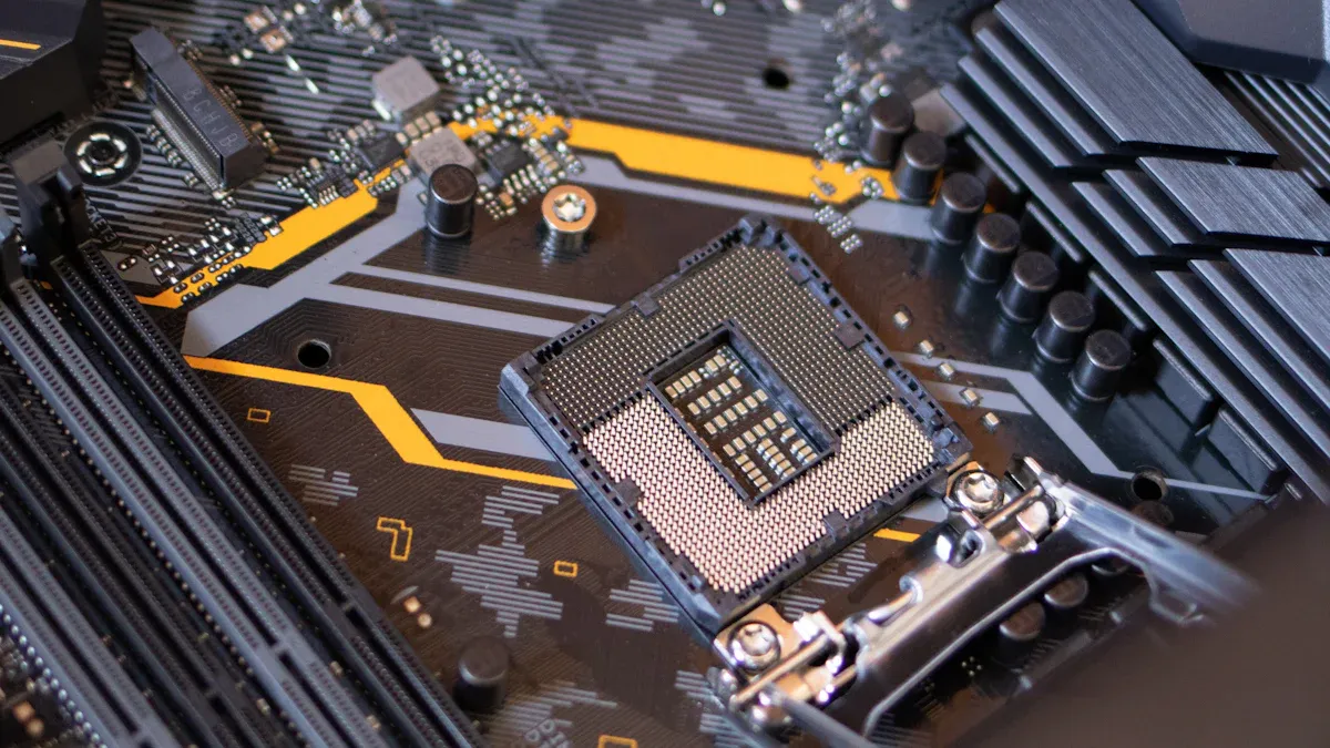
Electronics and Semiconductor Devices
Ceramic semiconductor materials play a vital role in the electronics industry. Their unique properties, such as thermal stability, electrical insulation, and mechanical strength, make them indispensable in semiconductor devices. These materials are used in substrates, insulators, and capacitors, ensuring reliable performance in high-power and high-frequency applications.
The table below highlights key performance benchmarks that demonstrate their effectiveness:
| Performance Benchmark | Description |
|---|---|
| Thermal Stability | Ceramics can withstand high temperatures, maintaining structural integrity in extreme conditions. |
| Electrical Insulation | Materials like alumina and zirconia provide excellent insulation, crucial for preventing electrical interference. |
| Mechanical Strength | High strength and hardness of ceramics ensure durability in manufacturing equipment, reducing wear and tear. |
These benchmarks underscore the critical role of ceramic semiconductor materials in advancing electronic technologies.
Aerospace Components
In aerospace, ceramic semiconductor materials are essential for components exposed to extreme conditions. Their high-temperature resistance and thermal shock tolerance make them ideal for turbine blades, heat shields, and engine parts. Silicon carbide, for example, is widely used in aerospace applications due to its ability to maintain structural integrity under intense thermal and mechanical stress.
Additionally, these materials contribute to weight reduction in aerospace designs. Their lightweight nature, combined with exceptional strength, enhances fuel efficiency and overall performance. This makes them a preferred choice for modern aerospace engineering.
Optics and Advanced Manufacturing
Ceramic semiconductor materials also find extensive use in optics and advanced manufacturing. Their optical transparency and dielectric properties make them suitable for lenses, mirrors, and laser components. Alumina and zirconia are commonly used in optical systems due to their ability to withstand high-energy environments without degradation.
In advanced manufacturing, these materials enhance the precision and durability of tools and equipment. Their hardness and wear resistance ensure long-lasting performance, reducing maintenance costs and downtime. This versatility highlights their importance in cutting-edge industrial applications.
Ceramic semiconductor materials represent a unique fusion of ceramic durability and semiconductor functionality, enabling their use in diverse industries. Their exceptional properties, such as thermal stability, electrical conductivity, and mechanical strength, make them indispensable in electronics, aerospace, and optics. These materials continue to drive innovation, supporting advancements in high-performance devices and sustainable manufacturing processes.
Long-term market trends underscore the growing demand for these advanced materials. Companies investing in innovative manufacturing techniques and forming strategic partnerships are well-positioned to meet evolving industry needs. This highlights the importance of sustained research and development to unlock the full potential of ceramic semiconductor technologies.
The future of ceramic semiconductor materials lies in their ability to adapt to emerging challenges, ensuring they remain at the forefront of technological progress.
FAQ
What makes ceramic semiconductor materials unique compared to traditional semiconductors?
Ceramic semiconductor materials combine high thermal stability, mechanical durability, and electrical conductivity. Unlike traditional semiconductors, they excel in extreme conditions, such as high temperatures or mechanical stress, making them ideal for aerospace, electronics, and industrial applications.
How are ceramic semiconductor materials processed to achieve high purity?
Manufacturers use advanced techniques like electron energy loss spectroscopy (EELS) and energy-filtered transmission electron microscopy (EFTEM). These methods ensure precise control over composition and structure, minimizing impurities and optimizing properties for high-performance applications.
Why is silicon carbide (SiC) widely used in power electronics?
Silicon carbide offers superior thermal conductivity and high-temperature resistance. These properties reduce heat generation and improve energy efficiency in power devices, making SiC essential for electric vehicles, renewable energy systems, and high-frequency applications.
Can ceramic semiconductor materials be used in optical systems?
Yes, materials like alumina and zirconia exhibit optical transparency and dielectric strength. These properties make them suitable for lenses, mirrors, and laser components, especially in high-energy environments requiring durability and precision.
What industries benefit most from ceramic semiconductor materials?
Electronics, aerospace, and optics benefit significantly. These materials enhance device reliability, reduce weight in aerospace designs, and improve precision in optical systems. Their versatility supports advancements in high-performance technologies across multiple sectors.