

Ceramic Sintering for Electronic Components
Ceramic sintering is a fundamental thermal process. It transforms powdered Ceramic Materials into dense, solid structures. This process is crucial for modern electronic components. Sintering creates high-performance materials from raw ingredients. The ceramic electronic components market reached an estimated US$ 11.6 Billion in 2023, with a projected 5.0% CAGR, underscoring its vital role in the electronics industry.
Key Takeaways
- Ceramic sintering turns ceramic powders into strong, solid parts. This process is vital for making modern electronic components.
- Sintering improves materials. It makes them denser, stronger, and better at conducting electricity or heat.
- Different sintering methods exist. Solid-state, liquid-phase, and pressure-assisted sintering each work in unique ways.
- Sintering helps electronic parts work better. It controls electrical properties like how much energy they store or how well they conduct.
- This process makes electronic components tough. They can handle heat changes and impacts, lasting longer.
- Sintering allows smaller electronics. It helps create tiny, multi-layered parts for compact devices.
- New sintering methods save energy. They also use eco-friendly materials, making electronics more sustainable.
Understanding Ceramic Sintering for Electronic Components
The Core Process of Ceramic Sintering
Powder Preparation and Compaction
The journey of ceramic sintering begins with meticulous powder preparation. Manufacturers carefully select and process raw ceramic materials. This often involves milling to achieve a uniform particle size distribution. After preparation, compaction forms the powders into a desired shape, known as a green body. Techniques like uniaxial pressing, isostatic pressing, or slip casting create these preliminary forms. The green body has sufficient strength for handling before the thermal treatment.
Thermal Treatment Stages
Thermal treatment is the heart of the Sintering Process. It involves heating the green body to high temperatures. For co-doped TiO2 ceramics, high-temperature sintering often exceeds 1400 °C. Fluoropolymers, like PTFE, require sintering temperatures above their melting point, typically ranging from 360 °C to 380 °C. Nanosized particles generally sinter at lower temperatures. For instance, nano yttrium stabilized zirconia (YSZ) begins sintering 200 °C lower than its conventional counterpart. The optimal sintering temperature range is often between 60% and 80% of the material's melting temperature, which translates to 1006 °C and 1342 °C for many ceramics. Controlled environments, such as vacuum, inert gases, or reducing atmospheres, prevent oxidation or unwanted chemical reactions during this stage.
Driving Forces of Sintering
Thermodynamic and kinetic principles drive the densification and microstructural evolution during sintering. Thermodynamic analysis helps understand changes in phase composition. For example, LiCO3 decomposition enhances densification in LLZTO ceramics during ultrafast high-temperature sintering (UHS). High heating rates, characteristic of UHS, make densification a more dominant behavior than grain growth. Increasing the heating rate can lead to finer pore structures. This occurs due to the competition between surface diffusion and the densification process. High heating rates also reduce grain coarsening, accelerating densification through enhanced grain boundary and volume diffusion.
Key Sintering Mechanisms for Electronic Components
Solid-State Sintering
Solid-state sintering involves the densification of ceramic powders without forming a liquid phase. Atomic diffusion is the primary mechanism. Atoms move across particle boundaries, filling pores and reducing the overall volume. This process relies on high temperatures to activate atomic movement.
Liquid-Phase Sintering
Liquid-phase sintering occurs when a small amount of liquid forms during heating. This liquid phase wets the solid particles, facilitating particle rearrangement and promoting faster densification. The liquid acts as a transport medium for material transfer, allowing particles to pack more efficiently.
Pressure-Assisted Sintering
Pressure-assisted sintering combines heat with external pressure. This technique enhances densification, often at lower temperatures or shorter times. Hot pressing and spark plasma sintering (SPS) are examples. Applying pressure helps overcome resistance to densification, leading to denser materials with finer microstructures.
Material Properties Enhanced by Sintering for Electronic Components
Density and Porosity Control
Sintering significantly increases the density of ceramic materials. It reduces porosity, which is crucial for achieving desired mechanical and electrical properties. A dense structure minimizes defects and improves overall performance.
Grain Size and Microstructure
Sintering controls the grain size and microstructure of the ceramic. Fine, uniform grain structures generally lead to superior mechanical strength and improved electrical properties. The sintering parameters dictate the final grain morphology.
Mechanical Strength and Hardness
The densification and microstructural control achieved through sintering directly enhance the mechanical strength and hardness of ceramic components. This makes them more robust and durable for demanding applications.
Electrical and Thermal Conductivity
Sintering plays a vital role in optimizing electrical and thermal properties.
| Material Property | Enhancement by Sintering |
|---|---|
| Dielectric Breakdown Strength (DBS) | Higher DBS achieved with dense microstructures in sintered reaction-bonded silicon nitride (Si3N4), influenced by sintering additives. |
| Thermal Conductivity | Sintering facilitates densification and phase transition in Si3N4 ceramics, leading to a dense, homogeneous, and non-porous microstructure, resulting in high thermal conductivity (e.g., 78.16 W/mK). |
| Dielectric Constant | Sintering processes and additives influence appropriate dielectric constants (e.g., 8.50 for Si3N4) for LTCC applications. |
| Dielectric Loss | Sintering processes and additives influence low dielectric loss (e.g., 5.52 × 10⁻⁴ for Si3N4) for LTCC applications. |
| Coefficient of Thermal Expansion | Sintering influences the thermal expansion coefficient of Li2SiO3-based ceramics, with an average coefficient reaching 15.7 × 10⁻⁶/K (at 100 °C). |
| These enhancements are critical for the reliable operation of various Electronic Components. |
Why Sintering is Critical for Electronic Component Performance
Sintering is an indispensable process for modern electronics. It directly influences the performance, reliability, and miniaturization capabilities of various electronic components. This thermal treatment transforms raw ceramic powders into functional materials with precise electrical, mechanical, and structural characteristics.
Achieving Desired Electrical Characteristics in Electronic Components
Sintering precisely tailors the electrical behavior of ceramic materials. This control is vital for components ranging from insulators to conductors.
Dielectric Constant and Loss Tangent
The dielectric constant (ε′) measures a material's ability to store electrical energy. The loss tangent (tanδ) indicates the energy dissipated as heat. Sintering processes optimize these properties, which are crucial for capacitors, insulators, and high-frequency applications. Optimized sintering conditions can yield materials with stable dielectric constants and minimal energy loss.
| Material | Sintering Conditions | Electrical Characteristics |
|---|---|---|
| TiO2 doped with Ta2O5 and indium tin oxides (ISO) | 1400 °C for 3 hours | Low loss tangent (0.007–0.04 at 103 Hz), high dielectric constant (∼2–4 × 10^4), temperature coefficient of ε′ at 1 kHz from −120 to 200 °C lower than ±10%, ε′ nearly independent of DC bias (even at 300 V/cm, ∼2.6%), ε′ nearly independent of humidity (25–90%RH) |
| In3+ and Nb5+ co-doped rutile TiO2 (InNbTO) | Not specified | Very high ε′ of 10^4, low tanδ of 0.02 over wide frequency and temperature ranges |
| (Al3+, Nb5+) co-doped CaCu3Ti4O12 ceramics | Not specified | High dielectric permittivities with good temperature stability |
| TiO2 co-doped with aliovalent Nb5+ and isovalent Sn4+ | Not specified | Improved temperature stability of dielectric properties |
These examples demonstrate how specific sintering parameters and material compositions lead to superior dielectric performance.
Resistivity and Conductivity
Resistivity measures a material's opposition to electrical current flow. Conductivity is the inverse, indicating how well a material conducts electricity. Sintering allows engineers to precisely control these properties, creating materials suitable for insulators, semiconductors, or conductors.
| Type | Resistivity Range (Ω·m) |
|---|---|
| Insulators | 10⁸ – 10¹⁷ |
| Semiconductors | 10⁻⁵ – 10⁶ |
| Conductors | 10⁻⁸ – 10⁻⁵ |
| Superconductors | Near 0 (below Tc) |
Alumina (Al₂O₃) exemplifies an excellent insulator. It exhibits a high electrical resistivity, typically around 10¹⁴ Ω·cm at room temperature. Its resistivity decreases with increasing temperature, but it maintains its highly insulating properties, for example, 10¹⁰ Ω·cm at 500°C. Sintering ensures the material achieves the necessary density and microstructure for these specific electrical roles.
Piezoelectric and Pyroelectric Properties
Sintering plays a crucial role in developing piezoelectric and pyroelectric ceramics. Piezoelectric materials generate an electric charge when subjected to mechanical stress. Pyroelectric materials produce an electric charge in response to temperature changes. Sintering processes optimize the crystal structure, grain orientation, and density of these ceramics. This optimization enhances their sensitivity and efficiency for applications in sensors, actuators, and transducers.
Enhancing Mechanical Reliability of Electronic Components
Electronic components often operate in demanding environments. Sintering significantly improves their mechanical robustness and reliability.
Withstanding Thermal Cycling
Electronic devices frequently experience temperature fluctuations. These changes cause materials to expand and contract, leading to thermal stress. Sintering creates dense, strong ceramic microstructures. These structures resist crack propagation and minimize internal stresses caused by thermal cycling. This resilience ensures the component's integrity and function over its operational lifespan.
Improving Impact Resistance
Sintering reduces porosity and increases the density of ceramic materials. This process directly enhances their toughness and impact resistance. Components with improved impact resistance can better withstand physical shocks and vibrations. This makes them suitable for applications in harsh environments or portable devices.
Ensuring Long-Term Stability
The long-term stability of electronic components is paramount for reliable operation. Sintering, particularly with advanced materials like Ag-coated Cu (Cu@Ag) particles, significantly enhances thermal reliability and operational lifespan. This process improves bond strength and mitigates oxidation, which are critical for power semiconductors operating at high temperatures. Experiments at 300 °C in inert and air atmospheres showed that applying pressure during sintering creates a denser microstructure. This denser structure restricts oxygen access and improves mechanical properties. Pressure-assisted sintering leads to higher initial shear strength and better resistance to thermal degradation. Thermal aging tests further demonstrated an increase in shear strength over time in sintered joints, reaching 57.9 MPa in an inert atmosphere and 42.0 MPa in air after 500 hours. This indicates enhanced mechanical stability under prolonged thermal exposure.
Enabling Miniaturization and Integration of Electronic Components
Modern electronics demand smaller, more powerful devices. Sintering is a key enabler for miniaturization and high-density integration.
High-Density Packaging
Sintering allows for the creation of ceramic substrates and packages with precise dimensions and excellent material properties. These properties include high thermal conductivity and electrical insulation. This precision enables high-density packaging, where multiple components integrate into a compact space. This reduces the overall size of electronic devices while maintaining or improving performance.
Multi-Layer Ceramic Devices
Sintering is fundamental to fabricating multi-layer ceramic devices, such as multi-layer ceramic capacitors (MLCCs) and multi-layer ceramic substrates. These devices stack multiple layers of ceramic and conductive traces, creating complex circuits in a compact form.
- Layer Lamination: For multi-layer designs, additional layers are laminated before the final sintering.
- Final Sintering: The entire assembly is sintered at 1500-1650°C to solidify the layers and form the finished circuit board.
- Co-Firing Process (LTCC): The entire assembly is co-fired at a lower temperature (around 850°C to 900°C) than traditional ceramic firing processes. This step ensures that all layers bond together and components are securely integrated without damage.
This multilayer capability enables complex circuit designs in a compact form factor, enhancing functionality and performance. Alumina is a preferred material for multi-layer ceramic packages due to its cost-effectiveness, excellent thermal and electrical properties, and ease of processing. Manufacturing techniques like pressing and sintering enable high-volume production and cost efficiency for alumina-based multi-layer ceramic packages. High-performance ceramic substrates, often made from materials like alumina, are crucial for surface mount package – leadless technology. This technology supports miniaturized, high-density, and high-reliability electronic assemblies, including dense multi-layer configurations. It provides precise thermal management, electrical insulation, and mechanical stability. Ceramics are essential for maintaining signal integrity and device reliability in these compact, multi-layer layouts. Research on multi-layer CGO membranes demonstrates the role of sintering in fabricating asymmetric porous/dense bi-layer structures. This involves tape casting, lamination, and co-sintering of compatible porous and dense CGO layers, indicating that sintering is a fundamental step in creating complex multi-layer ceramic devices.
Fine Feature Resolution
The demand for ever-smaller features in advanced electronics drives innovation in sintering techniques. Advanced methods achieve extremely fine resolutions, enabling the fabrication of micro-scale components and intricate circuit patterns.
| Metric | Value (μm) | Notes |
|---|---|---|
| Feature Resolution (μ-SLS) | < 5 | Achieved by novel microscale selective laser sintering |
| Pixel Resolution (μ-SLS) | ~1 | Achieved by novel microscale selective laser sintering |
| Line Width (μ-SLS) | 50 | For fabricated structures |
| Spacing (μ-SLS) | 50 | For fabricated structures |
| Average Height (1-layer μ-SLS) | 2.24 | For multilayer structures |
| Average Height (2-layer μ-SLS) | 3.98 | For multilayer structures |
| Average Height (3-layer μ-SLS) | 8.02 | For multilayer structures |
| RMS Height (2-layer rectangular pillars) | 5.77 | |
| Resolution (Conventional Macroscale SLS) | 70–100 | Limited by microscale powders and laser spot sizes |
| Diameter (SnAg bumps) | > 100 | Previous technology |
| Pitch (SnAg bumps) | > 150 | Previous technology |
| Diameter (Electroplated Copper Pillars) | < 100 | Previous technology |
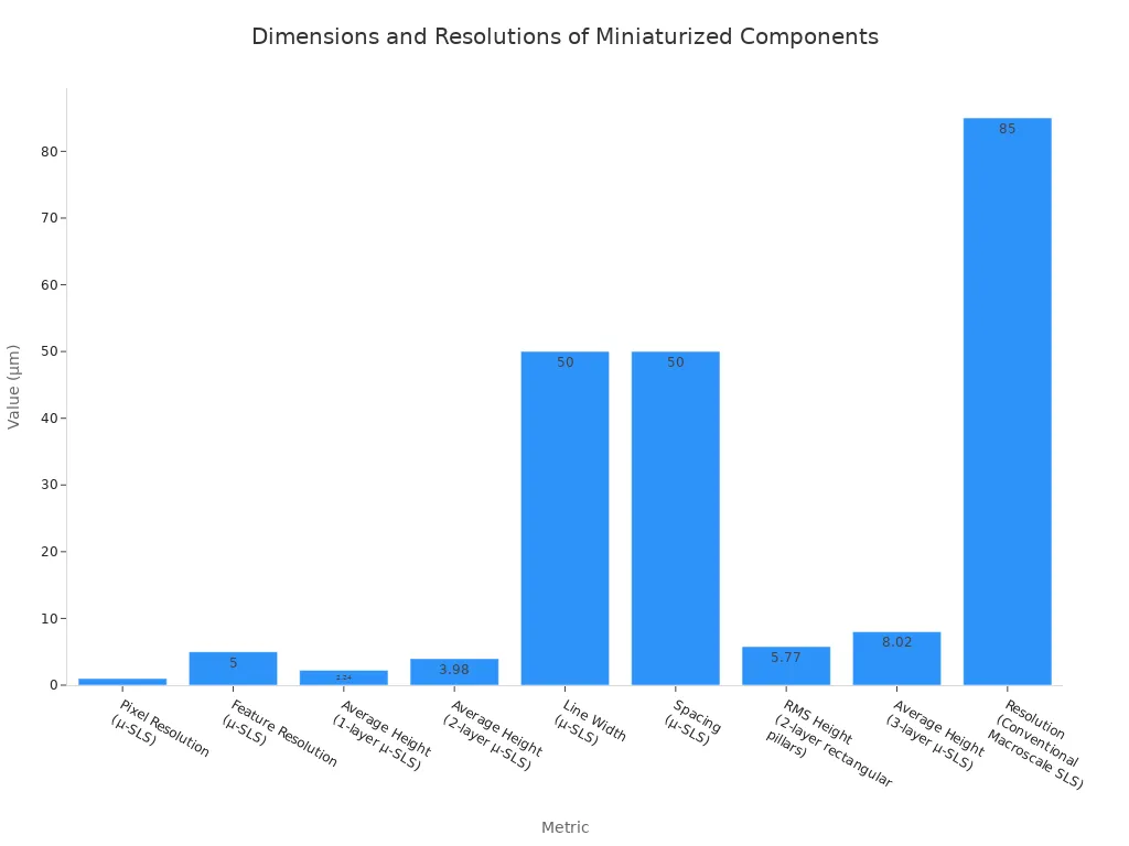
Microscale selective laser sintering (μ-SLS) exemplifies these advancements. It achieves feature resolutions as fine as 5 μm and pixel resolutions of approximately 1 μm. This capability is essential for creating the next generation of miniaturized and highly integrated electronic devices.
Sintering's Impact on Specific Electronic Components
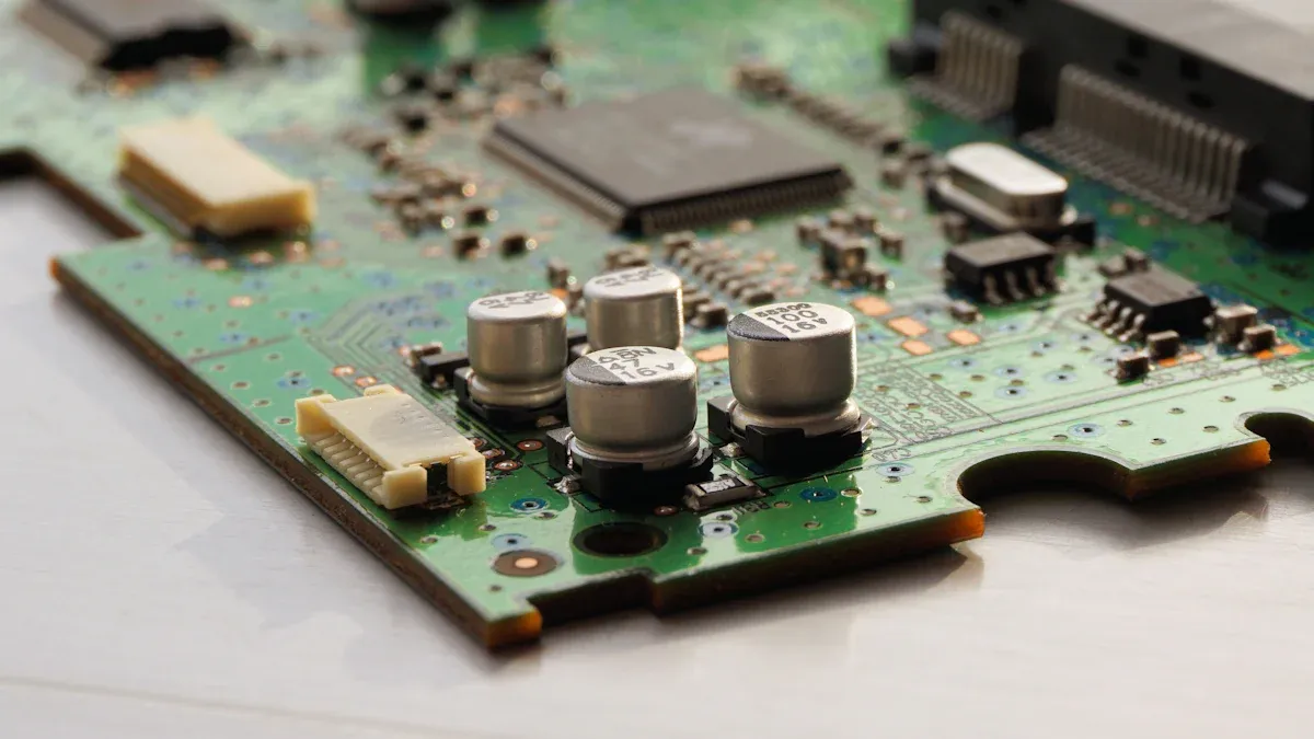
Sintering fundamentally shapes the performance and reliability of many electronic components. This thermal process transforms raw ceramic materials into functional parts with precise electrical, mechanical, and structural characteristics.
Ceramic Substrates and Packaging for Electronic Components
Sintering transforms ceramic powders into robust substrates and packaging. These materials provide critical support and protection for sensitive electronic components.
High Thermal Conductivity Substrates
Sintering creates dense ceramic substrates with excellent thermal conductivity. These substrates efficiently dissipate heat generated by integrated circuits, preventing overheating and ensuring reliable operation. Materials like alumina and aluminum nitride, when properly sintered, offer superior thermal management capabilities.
Hermetic Sealing for Protection
Manufacturers use sintering to form hermetic seals in ceramic packages. These seals create an airtight barrier, protecting delicate electronic components from moisture, dust, and other environmental contaminants. This protection significantly extends the lifespan and reliability of the devices.
Multi-Chip Module Applications
Sintered ceramic substrates are fundamental to multi-chip module (MCM) technology. MCMs integrate multiple bare semiconductor chips onto a single substrate. Sintering provides the necessary dimensional stability, electrical insulation, and thermal performance for these complex, high-density assemblies. This enables compact and powerful electronic systems.
Capacitors and Resistors as Electronic Components
Sintering precisely controls the electrical properties of ceramic materials, making it indispensable for manufacturing capacitors and resistors.
High-K Dielectric Capacitors
Sintering processes create ceramic materials with high dielectric constants (high-K dielectrics). These materials allow capacitors to store more electrical charge in a smaller volume. This is crucial for miniaturized electronic components. Careful control of sintering temperature and atmosphere optimizes the crystal structure, which directly influences the dielectric constant.
Thick Film Resistors
Sintering significantly influences the performance and stability of thick film resistors.
- Lowering the firing temperature from 850°C to 750°C substantially reduces interaction between the FGC substrate and the resistor layer. This reduction leads to thick-film resistors on FGC substrates with performance characteristics comparable to those on alumina substrates.
- The temperature coefficient of resistance (TCR) of the resistor helps assess how the substrate's coefficient of thermal expansion (CTE) influences the overall TCR. However, sintering can also negatively impact resistance stability. Thick-film resistors sintered on olivine gabbro showed increased sheet resistivity, approximately 30–50 kΩ/□. This increase was linked to cracking in the resistor layer, caused by residual stress that developed after the sintering process.
Miniaturized Chip Components
Sintering enables the mass production of miniaturized chip components, including chip resistors and chip capacitors. The process ensures precise dimensions, consistent electrical properties, and mechanical robustness for these tiny devices. This capability is vital for the compact design of modern electronics.
Sensors and Actuators as Electronic Components
Sintering plays a critical role in fabricating ceramic sensors and actuators, optimizing their functional properties for various applications.
Piezoelectric Transducers
Sintering processes are essential for creating high-performance piezoelectric ceramics. These materials convert mechanical energy into electrical energy and vice versa, making them ideal for transducers in medical imaging, sonar, and industrial sensors.
| Ceramic Type | Electromechanical Coupling Factor (k33) | Notes |
|---|---|---|
| State-of-the-art PZT ceramics | 65–78% | Compared to single crystals |
| Textured PIN-PSN-PT ceramics | 85–89% | High k33 and increased Trt (160-200°C) |
| Ceramic Type | Piezoelectric Coefficient (d33) | Electromechanical Coupling Factor (kp) | Notes |
|---|---|---|---|
| PZT-4%Pb(Mn,W,Sb,Nb)O3 | N/A | 0.56 | Excellent mechanical quality (Qm=2344) |
| 91%PZT–1%PNN-8%PMN | N/A | 0.55 | Optimized sintering at 1250°C, high Qm=2256 |
| BITWC2 | 31.1 pC/N | N/A | Moderate TC (651°C), large remnant polarization (12.2 μC cm−1) |
| BITWC2 (at 600°C) | 26.6 pC/N | N/A | Excellent thermal stability |
| BaTiO3 (porous scaffolds) | Decreases with increasing porosity | N/A | Porosity from 10% to 90% |
| These tables illustrate how sintering parameters and material compositions achieve specific piezoelectric coefficients and electromechanical coupling factors, crucial for transducer performance. |
Thermistors and Varistors
Sintering controls the microstructure and composition of ceramic materials used in thermistors and varistors. Thermistors exhibit resistance changes with temperature, while varistors show resistance changes with voltage. Precise sintering ensures the desired temperature or voltage response characteristics for these protective and sensing devices.
Gas and Humidity Sensors
Sintering optimizes the sensitivity and selectivity of ceramic gas and humidity sensors by controlling their porous microstructure.
- Optimizing the pore size distribution of porous alumina by varying pore former content and calcination temperature improves sensitivity to moisture. Porous ceramic samples with pore size distributions of 0.2–0.3 µm (maximum porosity percentage) showed maximum sensitivity in the humidity range of 50–100 ppm. The porous structure of alumina compacts, controlled by particle size, pore size, and distribution through varying pore former percentage and sintering temperature, was crucial for achieving maximum sensitivity in the 50–100 ppmv moisture range.
- Elevating electrode sintering temperature can increase the size of NiO particles and shorten the length of the three-phase boundary (TPB) in the sensitive electrode. The longest average length of the TPB, corresponding to the best sensitive response to NO gas, was observed in the sensitive electrode sintered at 1000 °C. These examples highlight how sintering parameters directly influence the sensor's ability to detect specific gases or humidity levels accurately.
Advanced RF and Microwave Electronic Components
Sintering plays a pivotal role in the development of advanced radio frequency (RF) and microwave components. These components operate at very high frequencies, demanding materials with exceptional electrical properties. Sintering processes precisely control the microstructure and density of ceramic materials. This control enables the creation of components with low signal loss, high quality factors, and stable performance across wide temperature ranges.
Low-Loss Dielectric Resonators
Engineers use low-loss dielectric resonators in various RF and microwave applications. These applications include filters, oscillators, and antennas. Sintering is critical for achieving the necessary material properties. It densifies ceramic powders, eliminating pores that scatter electromagnetic waves and cause signal loss. The process also controls grain growth and phase purity. This ensures a homogeneous microstructure, which minimizes dielectric losses and maximizes the quality factor (Q-factor) of the resonator. A high Q-factor indicates efficient energy storage with minimal dissipation. For example, barium magnesium tantalate (Ba(Mg1/3Ta2/3)O3) ceramics, when properly sintered, exhibit extremely low dielectric loss at microwave frequencies. This makes them ideal for high-performance resonators.
High-Frequency Filters
Sintering enables the fabrication of compact and highly efficient high-frequency filters. These ceramic filters replace larger, more traditional metallic filters in many applications. They offer superior performance in terms of size, weight, and frequency selectivity. Sintering precisely controls the dielectric constant and temperature coefficient of resonant frequency in the ceramic material. This allows filter designers to achieve sharp frequency cut-offs and stable operation over varying temperatures. Multi-layer ceramic filters, created through co-firing processes, integrate multiple resonant structures into a single, miniaturized package. This integration significantly reduces the overall size of RF modules.
Antenna Substrates
Antenna substrates require materials with specific dielectric properties and mechanical strength. Sintering provides these critical characteristics for ceramic antenna substrates. The process ensures a uniform and stable dielectric constant across the substrate. This uniformity is essential for predictable antenna performance and radiation patterns. Sintering also minimizes the dielectric loss tangent, which reduces signal attenuation within the substrate. This leads to more efficient antennas. Furthermore, the high mechanical strength and thermal stability achieved through sintering allow these substrates to withstand harsh operating environments. This makes them suitable for applications in telecommunications, radar systems, and satellite communications.
Advanced Sintering Techniques for Electronic Components
Advanced sintering techniques push the boundaries of ceramic material processing. These methods enable the creation of components with superior properties and intricate designs. They address the increasing demands of modern electronics for performance and miniaturization.
Field-Assisted Sintering Technologies
Field-assisted sintering technologies apply external fields during the thermal process. This enhances densification and microstructural control.
Spark Plasma Sintering (SPS)
Spark Plasma Sintering (SPS) offers significant advantages over traditional methods. It achieves rapid densification at lower temperatures.
- SPS solidifies powder in a shorter time and at a lower temperature than hot pressing.
- It produces a uniform, crack-free microstructure, even with high thermal gradients.
- SPS yields extremely high density for piezoelectric dielectric ceramic materials.
- It allows adjustment of grain size (50 nm to 50 mm). This achieves higher piezoelectric constants and energy storage density, expanding application ranges.
| Feature | Conventional Sintering | Spark Plasma Sintering (SPS) |
|---|---|---|
| Heating Rate | 5 to 10°C per minute (slow) | 100°C per minute (rapid) |
| Temperature Requirement | High external temperature | Low sintering temperature needed, with about 20–30% reduction |
| Processing Time | Several hours | Minutes |
| Material Properties | Significant grain growth and changes in microstructure, potentially degrading properties | Fine grain with minimal growth, preserves intrinsic properties and uniform structure |
SPS reduces sintering temperatures by 400–500°C compared to traditional solid-phase sintering. It also lowers temperatures by 100–200°C compared to hot pressing. Its fast heating rates, reaching tens to hundreds of degrees Celsius per minute, reduce thermal cycles. Sintering completes in 5–10 minutes, a significant reduction from several hours. This technique offers precise microstructural control during sintering. It finds use in electronics for fabricating components, especially for high-temperature applications.
Flash Sintering
Flash Sintering (FS) is a promising low-energy consolidation technique. It significantly reduces energy consumption. FS applies electric fields and heat simultaneously. This causes a sudden drop in electrical resistivity and internal heat generation by the Joule effect. Densification occurs within seconds.
FS reduces processing time and furnace temperatures compared to conventional sintering. This leads to increased throughput, productivity, and energy efficiency. FS heats ceramics by dissipating heat directly inside the material through an applied electrical field. It enables a high degree of microstructural control. This positively influences the performance of ceramic components. Control parameters in FS include frequencies (DC to GHz), rates of change of current, voltage, or power, and pulsed energy discharge. These parameters allow for repeatable and homogeneous production of fully dense ceramics. Non-linear current profiles are crucial for tailoring the microstructure of BaTiO3 ceramics. This leads to better densification and improved grain growth.
Low-Temperature Co-fired Ceramic (LTCC) for Electronic Components
Low-Temperature Co-fired Ceramic (LTCC) technology is vital for multi-layer electronic component fabrication. It offers significant advantages.
Advantages of LTCC Technology
LTCC materials offer dielectric properties comparable to PTFE. They surpass FR4 in high-frequency performance. LTCC enables embedding passive components within the multilayer stack. This capability is not available with PTFE. It is crucial for applications with rising operating frequencies, such as Bluetooth at 2.45 GHz and beyond. Insertion loss and dielectric constant are critical in these applications.
LTCC boasts higher thermal conductivity (2 W/m/k, potentially 50 W/m/k with vias) compared to organic materials (0.5 W/m/k). This aids in managing increased power dissipation. It features a low temperature coefficient of resonant frequency (Tf < 10 ppm/°C) for high frequency stability. This is significantly better than FR4 (80 ppm/°C). The thermal coefficient of expansion (TCE) closely matches silicon and gallium arsenide. This allows for direct chip attachment. LTCC withstands extreme temperatures (>500°C) and offers better thermal shock resistance than organic materials. This makes it suitable for demanding environments like automotive applications.
LTCC allows the use of low-resistivity conductor materials like silver and gold. This is due to low firing temperatures (around 850°C). It produces highly integrated, hermetic, and monolithic surface-mount devices. This enables mounting active components for miniature multifunction assemblies. LTCC results in compact, multilayer, three-dimensional designs. These designs are significantly smaller than traditional planar microwave components.
Applications in Wireless Communication
LTCC facilitates high-level integration. It combines components within a miniature package. This reduces the need for external parts. It offers inherent temperature stability, reducing the need for temperature compensation. LTCC provides good thermal conductivity and a low coefficient of thermal expansion (TCE) adapted to silicon and GaAs. It is highly suitable for multilayer modules and the integration of passive components (R, L, C) and cavities. LTCC is very robust against mechanical and thermal stress. It offers long-lasting hermeticity and stability. It enables a high degree of miniaturization with 3-D functions like cavities, stepped bonding planes, channels, and membranes. LTCC offers high frequency stability and ideal heat conduction across a wide temperature range (-100 °C to +200 °C).
Additive Manufacturing and Sintering of Electronic Components
Additive manufacturing, or 3D printing, revolutionizes the fabrication of complex ceramic structures. Sintering remains a critical post-processing step.
3D Printing of Ceramic Components
3D printing allows for the creation of intricate ceramic components with complex geometries. This includes micro-scale features and internal channels. Techniques like stereolithography, binder jetting, and material extrusion are adapted for ceramic slurries and powders. These methods enable rapid prototyping and customization.
Post-Processing Sintering Challenges
Post-processing sintering of 3D-printed ceramic components presents specific challenges.
- High Sintering Temperatures: Ceramic materials require high temperatures to achieve their final strength and functionality. This demands specialized and expensive printers capable of maintaining these conditions.
- Brittleness: Ceramics are inherently brittle. This leads to difficulties in handling and susceptibility to damage during post-processing. It necessitates careful optimization of printing parameters and post-processing methods.
- Complexity in Post-Processing: Extensive post-processing, including high-temperature sintering, is required to achieve desired material properties and dimensional accuracy. This adds to the complexity and cost of production.
- Precision and Reproducibility: Achieving high precision and reproducibility is challenging. This is due to the material's behavior during printing and sintering. Temperature and humidity variations impact the final product's dimensions and quality.
Nanomaterials and Sintering for Advanced Electronic Components
Nanomaterials offer transformative potential for advanced electronic components. Their unique properties at the nanoscale significantly influence sintering behavior and the final material characteristics.
Sintering Nanopowders
Sintering nanopowders presents distinct advantages. These ultra-fine particles possess a high surface area-to-volume ratio, which drives densification more effectively. Nanopowders, especially those with elevated activation energy, promote the preferential formation of sintered necks during the early stages of sintering. This mechanism accelerates the densification process. It shortens the material migration path and effectively restrains Ostwald ripening during liquid phase sintering. These combined effects lead to accelerated densification and significant grain refinement. Furthermore, using nanosized particles in high-melting-point metal powder-based sintered compacts increases relative density. It also facilitates sintering at lower temperatures due to a decrease in the material's effective melting point.
Achieving Ultra-Fine Microstructures
The unique sintering behavior of nanopowders directly contributes to achieving ultra-fine microstructures. The accelerated densification and restrained grain growth result in materials with very small, uniform grains. This fine microstructure enhances various properties crucial for advanced electronic components. Advanced sintering techniques, such as Spark Plasma Sintering (SPS), further enhance this capability. SPS produces dense compacts with fine grain sizes at relatively low temperatures and shorter sintering times. It achieves this through rapid heating and cooling rates, applying both pressure and an electric field to the powders. This process results in near-theoretical density and controlled microstructures. Such precise control over microstructure is essential for developing high-quality sputtering targets and other high-performance ceramic parts.
Future Trends and Challenges in Ceramic Sintering for Electronic Components
The field of ceramic sintering constantly evolves. It addresses new demands from advanced technologies and environmental concerns. Researchers focus on making sintering processes more efficient, sustainable, and adaptable for future applications.
Sustainable Sintering Practices for Electronic Components
The electronics industry increasingly prioritizes sustainability. Sintering processes are adapting to reduce their environmental footprint.
Energy Efficiency in Sintering
New sintering techniques aim to significantly lower energy consumption.
- Low-temperature sintering methods use specific additives, modified atmospheres, and optimized heating profiles. These methods reduce energy use while maintaining product microstructure and properties.
- Advanced equipment designs feature improved insulation, precise temperature control, and innovative heating methods like microwave and induction heating. These enhancements boost energy efficiency.
- Novel material compositions, such as nanostructured powders and composite materials, enable sintering at reduced temperatures. They achieve this by lowering the activation energy.
- Process optimization methods involve tailored heating/cooling profiles, controlled atmosphere compositions, and multi-stage sintering. These strategies minimize energy usage.
- Sintering aids and flux materials significantly lower sintering temperature requirements. They form liquid phases at grain boundaries and enhance diffusion rates.
These advancements offer substantial environmental benefits. They can reduce greenhouse gas emissions by 30-60% compared to conventional high-temperature sintering. They also minimize fossil fuel consumption, conserve water by 20-40%, and improve air quality by generating fewer airborne particulates. TDK's LTCC technology, for example, uses proprietary glass formulations with low melting points. This allows full densification at lower temperatures, reducing energy consumption and carbon emissions. A rapid, low carbon footprint approach for freeform manufacturing spatial ceramic composites combines layer-by-layer deposition, photothermal in-situ solidification, and self-sustaining ceramization. This method achieves consolidation with only 1920 J of energy, reducing consumption over 100-fold and CO2 emissions by an estimated 1000-fold.
Environmentally Friendly Materials
The development of sustainable materials is crucial for green electronics. Conductive nanoparticles of gold, silver, and copper are emerging as materials for inks in printed electronics. These inks often print on non-polluting substrates like paper, creating flexible electronic circuits known as conductive papers. This approach supports 'green economy' products, which are efficient, biodegradable, and offer advantages like accessibility, low cost, and flexibility. Recycled silver is another key environmentally friendly material. Its use in manufacturing silver sinter paste significantly reduces CO2-equivalent emissions by approximately 40% for one sintered power module. Sintering technology also offers a process-related sustainability benefit. It extends the lifetime of die-attach components, reportedly 17 times longer than common solder joints. This increased longevity reduces waste and resource consumption over time.
Sintering for Emerging Electronic Component Technologies
Sintering adapts to meet the unique material requirements of cutting-edge electronic component technologies.
Quantum Computing Components
Ceramics are vital in many quantum technologies. They offer properties like electrical insulation, vacuum compatibility, high temperature stability, low density, and favorable thermal expansion. These characteristics minimize disturbances to fragile quantum states. 3D printing overcomes limitations of traditional ceramic manufacturing, which is often slow, expensive, and limited in shapes. This enables faster and more cost-effective creation of intricate ceramic components for quantum devices. A case study shows 3D-printed ceramic housings miniaturizing a quantum sensor from the size of a microwave oven to that of a couple of pennies (15 grams). It maintains optical alignment stability under heat and mechanical stress. This technology is ready for deployment in real-world systems like optical wavemeters, quantum sensors, and quantum computers. It offers customizability and faster manufacturing due to 3D printing.
Advanced Medical Electronics
Sintering plays a crucial role in advanced medical electronics. It enables the creation of biocompatible ceramic components for implants, sensors, and diagnostic tools. Precise control over microstructure and density ensures the safety and long-term performance of these devices within the human body.
High-Power Electronics
High-power electronics demand materials with superior thermal management and electrical insulation. Photonic sintering (PS) is being explored for non-oxide ceramics in printed electronics. It offers a high-throughput and scalable approach. PS engineers ceramics with tailored optoelectronic, thermoelectric, and electrochemical properties. These properties are vital for flexible and printed electronics requiring high thermal stability and superior electrical performance. Challenges for PS include achieving homogeneous densification, managing thermal gradients that can cause cracking, and ensuring optimal optical absorption characteristics. Future research aims to integrate PS with additive manufacturing to fabricate complex, high-performance ceramic architectures.
Overcoming Sintering Challenges for Electronic Components
The advancement of ceramic sintering involves addressing several key challenges.
Defect Control and Mitigation
Controlling defects is paramount for component reliability. Sintering processes must minimize porosity, cracks, and undesirable grain growth. These defects can compromise mechanical strength and electrical performance. Advanced characterization techniques and process modeling help identify and mitigate defect formation.
Cost-Effective Production Methods
Making advanced ceramic sintering more accessible requires cost-effective production methods.
| Method | Relative Cost | Typical Use Case |
|---|---|---|
| Microwave Sintering | Medium | Fine ceramics, fast production |
| Cold Sintering | Low-Medium | Low-temp electronics, soft ceramics |
| Microwave sintering improves efficiency through rapid and uniform heating, energy savings, and finer grain size due to short processing times. Cold sintering is a low-energy solution. It offers low energy consumption, compatibility with hybrid materials, and integration with polymers or electronics. Additive manufacturing (3D printing) using stereolithography-based technology enables precise, efficient, and cost-effective production of complex ceramic geometries. Ceramic Injection Molding (CIM) is another cost-effective method for manufacturing complex ceramic components. It reduces waste, minimizes secondary operations, and scales economically. This allows manufacturers to lower production costs and enhance component quality. |
Standardization and Quality Assurance
Standardization and quality assurance are essential for widespread adoption. Developing consistent testing protocols and quality control measures ensures the reliability and performance of sintered ceramic components. This builds confidence in the technology across various industries.
Ceramic sintering remains an indispensable process for the evolution of modern electronics. It transforms raw materials into high-performance ceramics, enabling critical advancements. Key benefits include achieving miniaturization, enhancing reliability, and optimizing electrical and mechanical properties. The future holds continued innovation with advanced sintering techniques and sustainable practices. These will drive progress for emerging technologies in the electronics industry.
FAQ
What is ceramic sintering?
Ceramic sintering transforms powdered ceramic materials into dense, solid structures. This thermal process applies heat to compact green bodies. It creates high-performance materials from raw ingredients. Sintering is fundamental for modern electronic components.
Why is sintering crucial for electronic components?
Sintering is indispensable for electronic components. It precisely controls electrical, mechanical, and structural characteristics. This process enables miniaturization, enhances reliability, and optimizes performance. It transforms raw ceramic powders into functional materials.
How does sintering enhance material properties?
Sintering significantly improves material properties. It increases density and reduces porosity. This process controls grain size and microstructure. It also boosts mechanical strength, hardness, and electrical/thermal conductivity. These enhancements are critical for reliable electronic component operation.
What is the difference between solid-state and liquid-phase sintering?
Solid-state sintering densifies ceramic powders without forming a liquid phase. Atomic diffusion drives this process. Liquid-phase sintering involves a small amount of liquid during heating. This liquid wets particles, facilitating faster densification and material transfer.
How does sintering enable miniaturization in electronics?
Sintering enables miniaturization through high-density packaging. It creates ceramic substrates and multi-layer ceramic devices. This process allows complex circuits in compact forms. It also achieves fine feature resolution, essential for smaller, more powerful electronic devices.
What are the benefits of Spark Plasma Sintering (SPS)?
Spark Plasma Sintering (SPS) offers rapid densification at lower temperatures. It produces uniform, crack-free microstructures. SPS allows precise grain size adjustment. This technique achieves high density and preserves intrinsic material properties.
How does sintering contribute to sustainable electronics?
Sintering contributes to sustainable electronics through energy efficiency. New techniques reduce energy consumption. It also promotes environmentally friendly materials like recycled silver. Sintering extends component lifetimes, reducing waste and resource consumption.